The way we will discuss this concept in the following manner
- What is SetUp and Hold time?
- Definition of Setup and Hold.
- Setup and Hold Violation.
- How to calculate the Setup and Hold violation in a design?
I saw that lots of people are confused with respect to this concept. And the reason of this are
- They know the definition but don't know the origin or say concept behind Setup and Hold timing.
- They know the formula for calculating setup and hold violation but don't know how this formula come in picture.
- They become confuse by few of the terminology like capture path delay, launch path delay, previous clock cycle, current clock cycle, data path delay, slew, setup slew, hold slew, min and max concept, slowest path and fastest path, min and max corner, best and worst case etc during the explanation of Setup and Hold Timings/Violation.
I hope I can clarify your confusion. Let me explain this and if you face any problem let me know.
What is Setup and Hold time?
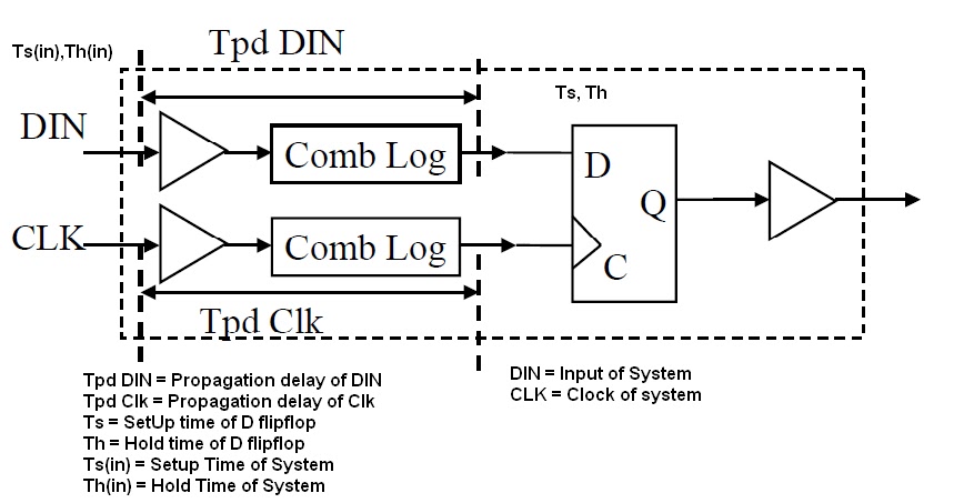
To understand the origin of the Setup and Hold time concepts first understand it with respect to a System as shown in the fig. An Input DIN and external clock CLK are buffered and passes through combinational logic before they reach a synchronous input and a clock input of a D flipflop (positive edge triggered). Now to capture the data correctly at D flip flop, data should be present at the time of positive edge of clock signal at the C pin ( to know the detail just read basis of D flipflop).
Note: here we are assuming D flip flop is ideal so Zero hold and setup time for this.
 |
| SetUp and Hold Time of a System |
There may be only 2 condition.
- Tpd DIN > Tpd Clk
- For capture the data at the same time when Clock signal (positive clock edge) reaches at pin C, you have to apply the input Data at pin DIN "Ts(in)=(Tpd DIN) - (Tpd Clk)" time before the positive clock edge at pin CLK.
- In other word, at DIN pin, Data should be stable "Ts(in)" time before the positive clock edge at CLK pin.
- This Time "Ts(in)" is know as Setup time of the System.
- Tpd DIN < Tpd Clk
- For capture the data at the same time when clock signal (positive clock edge) reaches at pin C, input Data at pin DIN should not change before "Th(in)= (Tpd Clk) - (Tpd DIN)" time. If it will change, positive clock edge at pin C will capture the next data.
- In other word, at DIN pin, Data should be stable "Th(in)" time after the positive clock edge at CLK pin.
- This time "Th(in)" is know as Hold Time of the System.
From the above condition it looks like that both the condition can't exist at the same time and you are right. But we have to consider few more things in this.
- Worst case and best case (Max delay and min delay)
- Because of environment condition or because of PVT, we can do this analysis for the worst case ( max delay) and best case ( min delay) also.
- Shortest Path or Longest path ( Min Delay and Max delay)
- If combinational logic has multiple paths, the we have to do this analysis for the shortest path ( min delay) and longest path ( max delay) also.
So we can say that above condition can be like this.
- Tpd DIN (max) > Tpd Clk (min)
- SetUp time == Tpd DIN (max) - Tpd Clk (min)
- Tpd DIN (min) < Tpd Clk (max)
- Hold time == Tpd Clk (max) - Tpd DIN (min)
For example for combinational logic delays are
Data path (max, min) = (5ns, 4 ns)
Clock path (max, min) = (4.5ns, 4.1ns)
Then Setup time= 5-4.1=0.9ns
Hold time is = 4.5-4=0.5ns
Now similar type of explanation we can give for a D flip flop. There is a combinational logic between C and Q , between D and Q of the Flipflop. There are different delays in those conbinational logic and based on there max and min value , a flipflop has Setup and Hold time. One circuitry of the positive edge triggered D flip is shown below.
 |
| Positive Edge Triggered D flip-flop |
There are different ways for making the D flip flop. Like by JK flipflop, master slave flipflop, Using 2 D type latches etc. Since the internal circuitry is different for each type of Flipflop, the Setup and Hold time is different for every Flipflop.
Definition:
Setup Time:
- Setup time is the minimum amount of time the data signal should be held steady before the clock event so that the data are reliably sampled by the clock. This applies to synchronous circuits such as the flip-flop.
- Or In short I can say that the amount of time the Synchronous input (D) must be stable before the active edge of the Clock.
- The Time when input data is available and stable before the clock pulse is applied is called Setup time.
Hold time:
- Hold time is the minimum amount of time the data signal should be held steady after the clock event so that the data are reliably sampled. This applies to synchronous circuits such as the flip-flop.
- Or in short I can say that the amount of time the synchronous input (D) must be stable after the active edge of clock.
- The Time after clock pulse where data input is held stable is called hold time.

Setup and Hold Violation:
In simple language-
If Setup time is Ts for a flip-flop and if data is not stable before Ts time from active edge of the clock, there is a Setup violation at that flipflop. So if data is changing in the non-shaded area ( in the above figure) before active clock edge, then it's a Setup violation.
And If hold time is Th for a flip flop and if data is not stable after Th time from active edge of the clock , there is a hold violation at that flipflop. So if data is changing in the non-shaded area ( in the above figure) after active clock edge, then it's a Hold violation.
Actually This am collecting for my self
ReplyDeletebecause if i will forget any blog name also
i can have the information here.So that's why