- Static Timing Analysis
- Dynamic Timing Analysis.
In this Blog (and few next as a part of this) we will discuss about the Static Timing Analysis. We will discuss Dynamic Timing Analysis later on.
Static Timing analysis is divided into several parts:
- Part1 -> Timing Paths
- Part2 -> Time Borrowing
- Part3a -> Basic Concept Of Setup and Hold
- Part3b -> Basic Concept of Setup and Hold Violation
- Part3c -> Practical Examples for Setup and Hold Time / Violation
- Part4 -> Delay
Note: Part 4, 5 and 6 are still under development.
Static Timing Analysis:
Static timing analysis is a method of validating the timing performance of a design by checking all possible paths for timing violations under worst-case conditions. It considers the worst possible delay through each logic element, but not the logical operation of the circuit.
In comparison to circuit simulation, static timing analysis is
- Faster - It is faster because it does not need to simulate multiple test vectors.
- More Thorough - It is more thorough because it checks the worst-case timing for all possible logic conditions, not just those sensitized by a particular set of test vectors.
Static timing analysis seeks to answer the question, “Will the correct data be present at the data input of each synchronous device when the clock edge arrives, under all possible conditions?”
In static timing analysis, the word static alludes to the fact that this timing analysis is carried out in an input-independent manner. It locates the worst-case delay of the circuit over all possible input combinations. There are huge numbers of logic paths inside a chip of complex design. The advantage of STA is that it performs timing analysis on all possible paths (whether they are real or potential false paths).
However, it is worth noting that STA is not suitable for all design styles. It has proven efficient only for fully synchronous designs. Since the majority of chip design is synchronous, it has become a mainstay of chip design over the last few decades.
The Way STA is performed on a given Circuit:
To check a design for violations or say to perform STA there are 3 main steps:
- Design is broken down into sets of timing paths,
- Calculates the signal propagation delay along each path
- And checks for violations of timing constraints inside the design and at the input/output interface.
Before we start all this we should know few key concepts in STA method: timing path, arrive time, required time, slack and critical path.
Let's Talk about these one by one in detail. In this Blog we will mainly Focus over Different Types of Timing Paths.
Timing Paths:
Timing paths can be divided as per the type of signals (e.g clock signal, data signal etc).
Types of Paths for Timing analysis:
- Data Path
- Clock Path
- Clock Gating Path
- Asynchronous Path
Start Point and End Point are different for each type of paths. It's very important to understand this clearly to understand and analysing the Timing analysis report and fixing the timing violation.
- Data path
- Start Point
- Input port of the design (because the input data can be launched from some external source).
- Clock pin of the flip-flop/latch/memory (sequential cell)
- End Point
- Data input pin of the flip-flop/latch/memory (sequential cell)
- Output port of the design (because the output data can be captured by some external sink)
- Clock Path
- Start Point
- Clock input port
- End Point
- Clock pin of the flip-flop/latch/memory (sequential cell)
- Clock Gating Path
- Start Point
- Input port of the design
- End Point
- Input port of clock-gating element.
- Asynchronous path
- Start Point
- Input Port of the design
- End Point
- Set/Reset/Clear pin of the flip-flop/latch/memory (sequential cell)
If we use all the combination of 2 types of Starting Point and 2 types of End Point, we can say that there are 4 types of Timing Paths on the basis of Start and End point.
- Input pin/port to Register(flip-flop).
- Input pin/port to Output pin/port.
- Register (flip-flop) to Register (flip-flop)
- Register (flip-flop) to Output pin/port
 |
| Timing Path- 4 types of Data Path |
PATH1- starts at an input port and ends at the data input of a sequential element. (Input port to Register)
PATH2- starts at the clock pin of a sequential element and ends at the data input of a sequential element. (Register to Register)
PATH3- starts at the clock pin of a sequential element and ends at an output port.(Register to Output port).
PATH4- starts at an input port and ends at an output port. (Input port to Output port)
Clock Path:
Please check the following figure
 |
| Timing Paths- Clock Paths |
In the above fig its very clear that for clock path the starts from the input port/pin of the design which is specific for the Clock input and the end point is the clock pin of a sequential element. In between the Start point and the end point there may be lots of Buffers/Inverters/clock divider.
Clock Gating Path:
Clock path may be passed trough a “gated element” to achieve additional advantages. In this case, characteristics and definitions of the clock change accordingly. We call this type of clock path as “gated clock path”.
As in the following fig you can see that
 |
| Timing Path- Clock Gating path. |
LD pin is not a part of any clock but it is using for gating the original CLK signal. Such type of paths are neither a part of Clock path nor of Data Path because as per the Start Point and End Point definition of these paths, its different. So such type of paths are part of Clock gating path.
Asynchronous path:
A path from an input port to an asynchronous set or clear pin of a sequential element.
See the following fig for understanding clearly.
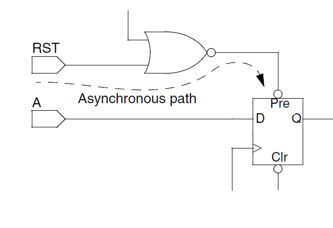 |
| Timing Path- Asynchronous Path |
As you know that the functionality of set/reset pin is independent from the clock edge. Its level triggered pins and can start functioning at any time of data. So in other way we can say that this path is not in synchronous with the rest of the circuit and that's the reason we are saying such type of path an Asynchronous path.
Other types of Paths:
There are few more types of path which we usually use during timing analysis reports. Those are subset of above mention paths with some specific characteristics. Since we are discussing about the timing paths, so it will be good if we will discuss those here also.
Few names are
- Critical path
- False Path
- Multi-cycle path
- Single Cycle path
- Launch Path
- Capture Path
- Longest Path ( also know as Worst Path , Late Path , Max Path , Maximum Delay Path )
- Shortest Path ( Also Know as Best Path , Early Path , Min Path, Minimum Delay Path)
Critical Path:
In short, I can say that the path which creates Longest delay is the critical path.
- Critical paths are timing-sensitive functional paths. because of the timing of these paths is critical, no additional gates are allowed to be added to the path, to prevent increasing the delay of the critical path.
- Timing critical path are those path that do not meet your timing. What normally happens is that after synthesis the tool will give you a number of path which have a negative slag. The first thing you would do is to make sure those path are not false or multicycle since it that case you can just ignore them.
False Path:
- Physically exist in the design but those are logically/functionally incorrect path. Means no data is transferred from Start Point to End Point. There may be several reasons of such path present in the design.
- Some time we have to explicitly define/create few false path with in the design. E.g for setting a relationship between 2 Asynchronous Clocks.
- The goal in static timing analysis is to do timing analysis on all “true” timing paths, these paths are excluded from timing analysis.
- Since false path are not exercised during normal circuit operation, they typically don't meet timing specification,considering false path during timing closure can result into timing violations and the procedure to fix would introduce unnecessary complexities in the design.
- There may be few paths in your design which are not critical for timing or masking other paths which are important for timing optimization, or never occur with in normal situation. In such case , to increase the run time and improving the timing result , sometime we have to declare such path as a False path , so that Timing analysis tool ignore these paths and so the proper analysis with respect to other paths. Or During optimization don't concentrate over such paths. One example of this. e.g A path between two multiplexed blocks that are never enabled at the same time. You can see the following picture for this.
 |
| False Path |
Here you can see that False path 1 and False Path 2 can not occur at the same time but during optimization it can effect the timing of another path. So in such scenario, we have to define one of the path as false path.
Same thing I can explain in another way (Note- Took snapshot from one of the forum). As we know that, not all paths that exist in a circuit are "real" timing paths. For example, let us assume that one of the primary inputs to the chip is a configuration input; on the board it must be tied either to VCC or to GND. Since this pin can never change, there are never any timing events on that signal. As a result, all STA paths that start at this particular startpoint are false. The STA tool (and the synthesis tool) cannot know that this pin is going to be tied off, so it needs to be told that these STA paths are false, which the designer can do by telling the tool using a "false_path" directive. When told that the paths are false, the STA tool will not analyze it (and hence will not compare it to a constraint, so this path can not fail), nor will a synthesis tool do any optimizations on that particular path to make it faster; synthesis tools try and improve paths until they "meet timing" - since the path is false, the synthesis tool has no work to do on this path.
Thus, a path should be declared false if the designer KNOWS that the path in question is not a real timing path, even though it looks like one to the STA tool. One must be very careful with declaring a path false. If you declare a path false, and there is ANY situation where it is actually a real path, then you have created the potential for a circuit to fail, and for the most part, you will not catch the error until the chip is on a board, and (not) working. Typically, false paths exists
- from configuration inputs like the one described above
- from "test" inputs; inputs that are only used in the testing of the chip,and are tied off in normal mode (however, there may still be some static timing constraints for the test mode of the chip)
- from asynchronous inputs to the chip (and you must have some form of synchronizing circuit on this input) (this is not an exhaustive list, but covers the majority of legitimate false paths).
MultiCycle Path:
- A multicycle path is a timing path that is designed to take more than one clock cycle for the data to propagate from the startpoint to the endpoint.
A multi-cycle path is a path that is allowed multiple clock cycles for propagation. Again, it is a path that starts at a timing startpoint and ends at a timing endpoint. However, for a multi-cycle path, the normal constraint on this path is overridden to allow for the propagation to take multiple clocks.
In the simplest example, the startpoint and endpoint are flops clocked by the same clock. The normal constraint is therefore applied by the definition of the clock; the sum of all delays from the CLK arrival at the first flop to the arrival at the D of the second clock should take no more than 1 clock period minus the setup time of the second flop and adjusted for clock skew.By defining the path as a multicycle path you can tell the synthesis or STA tool that the path has N clock cycles to propagate; so the timing check becomes "the propagation must be less than N x clock_period, minus the setup time and clock skew". N can be any number greater than 1.
Few examples are
- When you are doing clock crossing from two closely related clocks; ie. from a 30MHz clock to a 60MHz clock,
- Assuming the two clocks are from the same clock source (i.e. one is the divided clock of the other), and the two clocks are in phase.
- The normal constraint in this case is from the rising edge of the 30MHz clock to the nearest edge of the 60MHz clock, which is 16ns later. However, if you have a signal in the 60MHz domain that indicates the phase of the 30MHz clock, you can design a circuit that allows for the full 33ns for the clock crossing, then the path from flop30 -> to flop60 is a MCP (again with N=2).
- The generation of the signal 30MHZ_is_low is not trivial, since it must come from a flop which is clocked by the 60MHz clock, but show the phase of the 30MHz clock.
- Another place would be when you have different parts of the design that run at different, but related frequencies. Again, consider a circuit that has some stuff running at 60MHz and some running on a divided clock at 30MHz.
- Instead of actually defining 2 clocks, you can use only the faster clock, and have a clock enable that prevents the clocks in the slower domain from updating every other clock,
- Then all the paths from the "30MHz" flops to the "30MHz" flops can be MCP.
- This is often done since it is usually a good idea to keep the number of different clock domains to a minimum.
A Single-cycle path is a timing path that is designed to take only one clock cycle for the data to propagate from the startpoint to the endpoint.
Launch Path and Capture Path:
Both are inter-related so I am describing both in one place. When a flip flop to filp-flop path such as UFF1 to UFF3 is considered, one of the flip-flop launches the data and other captures the data. So here UFF1 is referred to "launch Flip-flop" and UFF3 referred to "capture flip-flop".

The Name "Launch path" referred to a part of clock path. Launch path is launch clock path which is responsible for launching the data at launch flip flop.
And Similarly Capture path is also a part of clock path. Capture path is capture clock path which is responsible for capturing the data at capture flip flop.
This is can be clearly understood by following fig.
 |
| Launch Clock Path (Launch Path) and Capture Clock Path (Capture path) |
Here UFF0 is referred to launch flip-flop and UFF1 as capture flip-flop for "Data path" between UFF0 to UFF1.So Start point for this data path is UFF0/CK and end point is UFF1/D.
One thing I want to add here (which I will describe later in my next blog- but its easy to understand here)-
- Launch path and data path together constitute arrival time of data at the input of capture flip-flop.
- Capture clock period and its path delay together constitute required time of data at the input of capture register.
 |
| Same clock path behave like Capture and Launch path for different Data path. |
Here you can see that for Data path1 the clock path through BUF cell is a capture path but for Data path2 its a Launch Path.
Longest and Shortest Path:
Between any 2 points, there can be many paths.
Longest path is the one that takes longest time, this is also called worst path or late path or a max path.
The shortest path is the one that takes the shortest time; this is also called the best path or early path or a min path.

I have tried my best to capture all the important points related to the Timing Paths. Please Let me know If anything is missing here.
No comments:
Post a Comment